• MOSI (Master Out Slave In)
• MISO (Master In Slave Out)
• SCK (Serial Clock)
• RESET
• GND (Ground)
Now connect the power supplies that are Vcc and GND to the micro controller.
Vcc = +5V and GND = 0V
Do not forget to connect Reset to Vcc with a 1K/10K resistor for pulling up. That is it we are ready with the hardware.
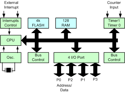
ATmega16 has 16 KB programmable flash memory, static RAM of 1 KB and EEPROM of 512 Bytes.
Pin No.
|
Pin name
|
Description
|
Alternate Function
|
1
|
(XCK/T0) PB0
|
I/O PORTB, Pin 0
|
T0: Timer0 External Counter Input.
XCK : USART External Clock I/O
|
2
|
(T1) PB1
|
I/O PORTB, Pin 1
|
T1:Timer1 External Counter Input
|
3
|
(INT2/AIN0) PB2
|
I/O PORTB, Pin 2
|
AIN0: Analog Comparator Positive I/P
INT2: External Interrupt 2 Input
|
4
|
(OC0/AIN1) PB3
|
I/O PORTB, Pin 3
|
AIN1: Analog Comparator Negative I/P
OC0 : Timer0 Output Compare Match Output
|
5
|
(SS) PB4
|
I/O PORTB, Pin 4
|
In System Programmer (ISP)
Serial Peripheral Interface (SPI)
|
6
|
(MOSI) PB5
|
I/O PORTB, Pin 5
| |
7
|
(MISO) PB6
|
I/O PORTB, Pin 6
| |
8
|
(SCK) PB7
|
I/O PORTB, Pin 7
| |
9
|
RESET
|
Reset Pin, Active Low Reset
| |
10
|
Vcc
|
Vcc = +5V
| |
11
|
GND
|
GROUND
| |
12
|
XTAL2
|
Output to Inverting Oscillator Amplifier
| |
13
|
XTAL1
|
Input to Inverting Oscillator Amplifier
| |
14
|
(RXD) PD0
|
I/O PORTD, Pin 0
|
USART Serial Communication Interface
|
15
|
(TXD) PD1
|
I/O PORTD, Pin 1
| |
16
|
(INT0) PD2
|
I/O PORTD, Pin 2
|
External Interrupt INT0
|
17
|
(INT1) PD3
|
I/O PORTD, Pin 3
|
External Interrupt INT1
|
18
|
(OC1B) PD4
|
I/O PORTD, Pin 4
|
PWM Channel Outputs
|
19
|
(OC1A) PD5
|
I/O PORTD, Pin 5
| |
20
|
(ICP) PD6
|
I/O PORTD, Pin 6
|
Timer/Counter1 Input Capture Pin
|
21
|
PD7 (OC2)
|
I/O PORTD, Pin 7
|
Timer/Counter2 Output Compare Match Output
|
22
|
PC0 (SCL)
|
I/O PORTC, Pin 0
|
TWI Interface
|
23
|
PC1 (SDA)
|
I/O PORTC, Pin 1
| |
24
|
PC2 (TCK)
|
I/O PORTC, Pin 2
|
JTAG Interface
|
25
|
PC3 (TMS)
|
I/O PORTC, Pin 3
| |
26
|
PC4 (TDO)
|
I/O PORTC, Pin 4
| |
27
|
PC5 (TDI)
|
I/O PORTC, Pin 5
| |
28
|
PC6 (TOSC1)
|
I/O PORTC, Pin 6
|
Timer Oscillator Pin 1
|
29
|
PC7 (TOSC2)
|
I/O PORTC, Pin 7
|
Timer Oscillator Pin 2
|
30
|
AVcc
|
Voltage Supply = Vcc for ADC
| |
31
|
GND
|
GROUND
| |
32
|
AREF
|
Analog Reference Pin for ADC
| |
33
|
PA7 (ADC7)
|
I/O PORTA, Pin 7
|
ADC Channel 7
|
34
|
PA6 (ADC6)
|
I/O PORTA, Pin 6
|
ADC Channel 6
|
35
|
PA5 (ADC5)
|
I/O PORTA, Pin 5
|
ADC Channel 5
|
36
|
PA4 (ADC4)
|
I/O PORTA, Pin 4
|
ADC Channel 4
|
37
|
PA3 (ADC3)
|
I/O PORTA, Pin 3
|
ADC Channel 3
|
38
|
PA2 (ADC2)
|
I/O PORTA, Pin 2
|
ADC Channel 2
|
39
|
PA1 (ADC1)
|
I/O PORTA, Pin 1
|
ADC Channel 1
|
40
|
PA0 (ADC0)
|
I/O PORTA, Pin 0
|
ADC Channel 0
|
Port A (PA7 ‐ PA0): Port A serves as the analog inputs to the A/D Converter. Port A also serves as an 8‐bit bi‐directional I/O port, if the A/D Converter is not used. When pins PA0 to PA7 are used as inputs and are externally pulled low, they will source current if the internal pull‐up resistors are activated. The Port A pins are tri‐stated when a reset condition becomes active, even if the clock is not running.
Port B (PB7 ‐ PB0): Port B is an 8‐bit bi‐directional I/O port with internal pull‐up resistors (selected for each bit). Port B also serves the functions of various special features of the ATmega16 as listed on page 58 of datasheet.
Port C (PC7 ‐ PC0): Port C is an 8‐bit bi‐directional I/O port with internal pull‐up resistors (selected for each bit). Port C also serves the functions of the JTAG interface and other special features of the ATmega16 as listed on page 61 of datasheet. If the JTAG interface is enabled, the pull‐up resistors on pins PC5(TDI), PC3(TMS) and PC2(TCK) will be activated even if a reset occurs.
Port D (PD7 ‐ PD0): Port D is an 8‐bit bi‐directional I/O port with internal pull‐up resistors (selected for each bit). Port D also serves the functions of various special features of the ATmega16 as listed on page 63 of datasheet.
RESET: Reset Input. A low level on this pin for longer than the minimum pulse length will generate a reset, even if the clock is not running.
XTAL1: External oscillator pin 1
XTAL2: External oscillator pin 2
41
AVCC: AVCC is the supply voltage pin for Port A and the A/D Converter. It should be externally connected to VCC, even if the ADC is not used. If the ADC is used, it should be connected to VCC through a low‐pass filter.
AREF: AREF is the analog reference pin for the A/D Converter.
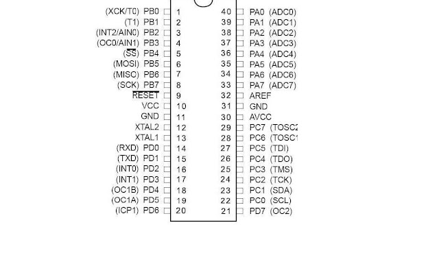
You can see it has 32 I/O (Input/output) pins grouped as A, B, C & D with 8 pins in each group. This group is called as PORT.
• PA0 ‐ PA7 (PORTA)
• PB0 ‐ PB7 (PORTB)
• PC0 ‐ PC7 (PORTC)
• PD0 ‐ PD7 (PORTD)
Notice that all these pins have some function written in bracket. These are additional function that pin can perform other than I/O. Some of them are.
• ADC (ADC0 ‐ ADC7 on PORTA)
• UART (Rx,Tx on PORTD)
• TIMERS (OC0 ‐ OC2)
• SPI (MISO, MOSI, SCK on PORTB)
• External Interrupts (INT0 ‐ INT2)