2012 | EMBEDDED AND ROBOTICS

Communication


Communication refers to the interaction between two devices in embedded system. It can be between computer and microcontroller or between two microcontrollers. 

Data Transfer

There are many techniques , different data transfer technique are used in different situations. Some example of data transfer is
Simple parallel transferUsed to transfer 8, 16, and 32 etc bits of data in the same time.
Asynchronous Serial Transfer (USART) –It is an old but still in use mode of serial communication uses only 2 lines (+1 additional line for GND).
SPI - Serial Peripheral Interface It is a standard mode of communication between different
ICs.
USB - A very advance, high speed and complicated serial Bus used in PCs to connect almost anything to it. 


Classification

Modes of Data Transfer can be divided into two types:
1. PARALLEL TRANSFER In this mode a number of bits (say 8,16 or 32) are transferred at a time. Thus they require as many electrical line as the number of bits to be transferred at once.

2. SERIAL TRANSFER In this mode only one bit is transfer at once. So to transfer 8 bits, 8 cycles are required.

Modes of Data Transfer can also be divided into
1. SYNCHRONOUS TRANSMISSION.
2. ASYNCHRONOUS TRANSMISSION

____________________________________________________________________________


Baud Rate
Baud Rate is a measurement of transmission speed in asynchronous communication. Devices that allow the communication must all agree on a single speed of information its unit is  'bits per second'.
 ____________________________________________________________________________

Summery

Transmission
Advantages
Disadvantages
Asynchronous
Simple & Inexpensive
High Overhead
Synchronous
Efficient
Complex and
Expensive


____________________________________________________________________________

Different Communication Techniques
Simplex : one sided communication like radio
Half duplex: like walkie talkie
Full duplex : video conferencing

Timers


Timer is an 8 bit register that keeps on increasing its value, so one of the basic conditions is the situation when timer register OVERFLOWS i.e. it has counted up to its maximum value (255 for 8 BIT timers) and rolled back to 0. In this situation timer can issue an interrupt and you must write an Interrupt Service Routine (ISR) to handle the event. There are three different timers available in Atmega16 and all the timers work in almost same way. They are TIMER0, TIMER1 and TIMER2.


TIMER MICROCONTROLLER 


Prescalar
The Prescalar is a mechanism for generating clock for timer by CPU clock.
Atmega has clocks of several frequencies such as 1 MHz, 8 MHz, 12 MHz, 16 MHz (max). The Prescalar is used to divide this clock frequency and produce a clock for TIMER. The Prescalarcan be set to produce the following types of clocks:
No Clock(Timer stop)
No prescaling (clock frequency = CPU frequency) FCPU/8
FCPU/64
FCPU/256
FCPU/1024
External clock


Timer Mode

Timers are usually used in one of the following modes:
Normal
CTC
Fast PWM
Phase correct PWM


Normal Mode

NORMAL MODE TIMERA timer running in normal mode will count up to its maximum value. When it reaches this maximum value, it issues an Overflow interrupt and resets the value of the timer to its original value.


In the above case, you can see that the time period is 256 times the time period of the clock. 255 clock cycles are required to attain the maximum value and one clock cycle to clear the timer value.
So, ftimer = fclock / 256
this mode has its limitations. We are confined to a very small set of values of frequency for the timer. This limitation is overcome by the compare mode.

CTC Mode
(clear timer on compare match)
Compare mode makes use of a register known as the Output Compare Register which stores a value of our choice. The timer continuously compares its current value with the value on the register and when the two values match, the timer resets itself to 0.
CTC mode timerIn that case, the output pin will remain high for one time period of the timer and will remain low for another time period. 


So,
tout = 2 * ttimer
From the normal case, we can draw an analogy to find out ttimer.
ttimer = tclock * (OCR + 1)
So, finally, we have the frequency as,
fout = fclock / (2 * (OCR + 1) )


Pulse Width Modulation (PWM) Mode
if you want to control the brightness of an LED (or any lamp), or the speed of DC motor, then digital on/off signals will not suffice. This situation is very smartly handled by a technique called as PWM or Pulse Width Modulation.

PWM is the technique used to generate analog signals from a digital device like a MCU.
In AVR microcontrollers, PWM signals are generated by timers. There are two methods by which you can generate PWM from timers:
1. Fast PWM
2. Phase Correct PWM


1.Fast PWM
Now for PWM generation from this count sequence OCR0 (Output Compare Register Zero) is used (Zero because it is for TIMER0 and there are more of these for TIMER1 & TIMER2). We can store any value between 0255 in OCR0, say we store
64 in OCR0 then it would appear in the graph as follows (the RED line).
Fast PWM timersWhen the TIMER0 is configured for fast PWM mode, then, while the timer is counting up, whenever the value of TIMER0 counter matches the value in the OCR0 register, an output PIN is pulled low (0) and when counting sequence begin again from 0 it is SET again (pulled high=VCC). This PIN is named OC0 and you can find it in the PIN configuration of ATmega
From the figure, you can see that a wave of duty cycle of 64/256 = 25% is produced by setting OCR0 to 64. You can set OCR0 to any value and get a PWM of duty cycle of (OCR0 / 256). When you set it to 0 you get a 0% duty cycle while setting it to 255 will give you a 100% duty cycle output. Thus by varying duty cycle you can get an analog voltage output from the OC0 PIN.
In the inverting mode the value of the OC0 pin is just the reverse of that in the above figure.


2.
Phase Correct PWM Mode
This mode is very similar to the Fast PWM mode except that whenever the value of the timer reaches its maximum value then instead of clearing the value of the timer it simply starts counting down.
 Phase Correct PWM Mode timer 


Overview of timers
timer 0 timer 1 timer 2 difference atmega


SETTING TIMERS IN CVAVR :

timer in cvavr

Assignment on ADC

MAKE PROGRAMS:


  1. GLOW LED ACCORDING TO  INPUT TO ADC
    0-99       1 LED
100-150      2LED
151-200      3 LED
200-255      4LED


2.  MAKE  DIGITAL VOLTMETER 
3.  MAKE DIGITAL WATTMETER


see answer here

ADC Analog to Digital convertor

What we have seen till now that the input given to uC was digital, i.e., either +5 V (logic 1) or 0V (logic 0). But what if we have an analog input, i.e., value varies over a range, say 0V to +5V? Then we require a tool that converts this analog voltage to discrete values. Analog to Digital Converter (ADC) is such a tool.


ADC is available at PORTA of Atmega16.
CLICK HERE FOR PIN DIAGRAM
Thus we have 8 pins available where we can apply analog voltage and get corresponding digital values. The ADC register is a 10 bit register, i.e., the digital value ranges from 0 to 1023. But we can also use only 8 bit out of it (0 to 255) as too much precision is not required.
Reference voltage is the voltage to which the ADC assigns the maximum value (255 in case of 8 bit and 1023 for 10 bit). Hence, the ADC of Atmega16 divides the input analog voltage range (0V to Reference Voltage) into 1024 or 256 equal parts, depending upon whether 10 bit or 8 bit ADC is used. For example, if the reference voltage is 5V and we use 10bit ADC, 0V has digital equivalent 0,
+5V is digitally 1023 and 2.5V is approximately equal to 512.

ADC =Vin x 255/Vref (8 bit)
ADC =Vin x 1023/Vref (10 bit)

Function:


read_adc()
This function returns the digital value of analog input at that pin of PORTA whose number is passed as parameter, e.g., if you want to know the digital value of voltage applied at PA3, and then just call the function as,
read_adc(3);
If the ADC is 8 bit, it will return a value from 0 to 255. Most probably you will need to print it on LCD. So, the code would be somewhat like


int a; char c[10]; // declare in the section of global variables
a=read_adc(3);
itoa(a,c);
lcd_puts(c);

SETTING UP ADC:
FOR OLDER VERSION OF CVAVR:

CVAVR ADC ANALOG TO DIGITAL CONVERTOR


FOR NEWER VERSION OF CVAVR:
CVAVR ADC ANALOG TO DIGITAL CONVERTOR

click here for projects on adc

Getting Started With Proteus : simulation software


PROTEUS ISIS adding components like microcontroller lcd and switchadding microcontroller

PROTEUS ISIS adding components like microcontroller lcd and switch


adding lcd
PROTEUS ISIS adding components like  lcd


PROTEUS ISIS adding components like  lcd  makin connections


adding hex file in microcontroller using proteus


adding hex file in microcontroller using proteus

to add switch, search for "button"
setting adc with proteus
led pattern circuit with proteus

Assignment on Pograms for lcd


1) Print a character on lcd
2) Print your name
3) Print a to z
4) Blink a character on lcd
5) Print a b c d…z  on only 1 coordinate after delay of 100ms
6) Moving name
7) Print name on pressing switch
8)  Make clock
9) Make calendar: having condition of leap year and leap year of century, each month having appropriate days.


Getting Started With CVAVR


new embedded project using cvavr


new embedded project using cvavr using atmega


new embedded project using cvavr


programming using cvavr


if you want to interface lcd also:

lcd interfacing using cvavr


ASSIGNMENT 1 -CONTROLLING LEDs

questions:


  1. GLOW A SINGLE LED
  2. GLOW 8 LED OF A PORT
  3. BLINKING A SINGLE LED
  4. BLINKING  8 LED OF A PORT
  5. ALTERNATE GLOWING LED s 
  6. GLOWING LED IN INCREASING PATTERN
  7. GLOWING LED IN DECREASING PATTERN
  8. GLOWING LED IN CONVERGING PATTERN
  9. GLOWING LED IN DIVERGING PATTERN
  10. BOTH CONVERGING AND DIVERGING PATTERN
  11. INCREASING AND DECREASING PATTERN
  12. WITH A SWITCH GLOW 1 LED
  13. WITH A SWITCH GLOW ALL 8 LEDS
  14. WITH 4 DIFFERENT SWITCH GLOW 4 DIFFERENT PATTERN
  15. WITH 1 SWITCH GLOW 4 DIFFERENT PATTERN 

1ST TRY YOURSEELF

Introducing DELAY


INTRODUCES TIME DELAY IN PARTICULAR STEP.


header file required : #include<delay.h>
syntax: delay_ms(200);               // where delay is 200 milli seconds 

Interfacing an LCD

Lcd

a 16 pin lcd have following pin connection
16*2 lcd

pin diagram and explanation of 16*2 lcd

Printing Functions
Now once the connections have been made, we are ready to display something on our screenSome of the general LCD functions which you must know are:

lcd_clear()
Clears the lcd. Remember! Call this function before the while(1) loop, otherwise you won’t be able to see anything!

lcd_gotoxy(x,y)
Place the cursor at coordinates (x,y) and start writing from there. The first coordinate is (0,0). Hence, x ranges from 0 to 15 and y from 0 to 1 in our LCD.
Example: you want to display something starting from the 5th character in second line, then the function would be
lcd_gotoxy(5,1);

lcd_putchar(char c)
To display a single character.
E.g.,
lcd_putchar(‘H’);

lcd_putsf(constant string)
To display a constant string.
Eg,
lcd_putsf(“IIT Kanpur”);

lcd_puts(char arr)
To display a variable string, ie an array of characters (data type char) in C language .
 e.g., You have an array char c[10] which keeps on changing. Then to display it, the function would be called as
lcd_puts(c);


Now we have seen that only characters or strings (constant or variable) can be displayed on the LCD. But quite often we have to display values of numeric variables, which is not possible directly. Hence we need to first convert that numeric value to a string and then display it. For e.g., if we have a variable of type integer, say int k, and we need to display the value of k (which changes every now and then, 200 now and 250 after a second... and so on). For this, we use the C functions itoa() and ftoa(), but remember to include the header file <stdlib.h> to use these C functions.


 itoa(int val, char arr[])
It stores the value of integer val in the character array arr. E.g., we have already defined int i and char c[20], then
itoa(i,c);
lcd_puts(c);
Similarly we have

ftoa(float val, char decimal_places, char arr[])
It stores the value of floating variable f in the character array arr with the number of decimal places as specified by second parameter. E.g., we have already defined float f and char c[20], then
ftoa(f,4,c); // till 4 decimal places
lcd_puts(c);

Now we are ready to display anything we want on our LCD. Just try out something which you would like to see glowing on it!


header file required : #include<lcd.h>   //but it is not required as it is already applied by cvavr by selecting lcd

HOW TO SELECT LCD:
get started with lcd on cvavr

adding lcd on cvavr

Registers - DDR , PORT , PIN

All the configurations in microcontroller is set through 8 bit (1 byte) locations in RAM (RAM is a bank of memory bytes) of the microcontroller called as Registers.

Input Output functions are set by Three Registers for each PORT.
• DDRX (DATA DIRECTION REGISTER)‐‐‐‐> Sets whether a pin is Input or Output of PORTX.
• PORTX ‐‐‐> Sets the Output Value of PORTX.
• PINX ‐‐‐‐‐> Reads the Value of PORTX.

DDR:  

First of all we need to set whether we want a pin to act as output or input. DDRX register sets this.

• To make Input set bit 0
• To make Output set bit 1

example  DDRB=11010001
(PORT‐B)
PB7   Output     1
PB6   Output     1
PB5   Input       0
PB4   Output     1
PB3   Input       0
PB2   Input       0
PB1   Input       0
PB0   Output     1


to make a whole 8 bit port as input or output:
DDRA=255   (FOR OUTPUT PORT: 255 IS USED AS IT IS 8PIN ie  8 BIT PORT{2^8})
DDRA=0       (FOR MAKING INPUT PORT)

To make an individual pin of port as input or output:
syntax    DDRA.X=0;  (INPUT)               // WHERE X IS THE PIN NO. starting from 0 to 7
             DDRA.X=1;  (OUTPUT)

example: DDRC.5=1;                //IT MAKES 5TH PIN OF PORT C AS OUTPUT PIN
-----------------------------------------------------------------------------------------------------------------------

PORT:

  This register sets the value to the corresponding PORT. Now a pin can be Output or Input. So let’s discuss both the cases.

• Output Pin
If a pin is set to be output, then by setting bit 1 we make output High that is +5V and by setting bit 0 we make output Low that is 0V.

SYNTAX:
PORTX ‐‐‐‐> to set value of PORTX with a byte.
PORTX.y ‐‐> to set value of yth pin of PORTX with a bit (works only with CVAVR)

example: PORTA.4=0;                       //GIVE 0 VOLT AT OUTPUT OF PIN 4 OF PORT A
PORTB=255;                             //GIVE 5 VOLT AT OUTPUT OF ALL PINS OF PORT B


• Input Pin

If a pin is set to be input, then by setting its corresponding bit in PORTX register will make it as follows, Set bit 0 ‐‐‐> Tri‐Stated Set bit 1 ‐‐‐> Pull Up
Tristated means the input will hang (no specific value) if no input voltage is specified on that pin.
Pull Up means input will go to +5V if no input voltage is given on that pin. It is basically connecting
PIN to +5V through a 10K Ohm resistance.
----------------------------------------------------------------------------------------------------------------------

PIN register:


This register is used to read the value of a PORT. If a pin is set as input then corresponding bit on PIN register is,
• 0 for Low Input that is V < 2.5V
• 1 for High Input that is V > 2.5V (Ideally, but actually 0.8 V ‐ 2.8 V is error zone!)

SYNTAX:

• PINX ‐‐‐‐> Read complete value of PORTX as a byte.
• PINX.y ‐‐> Read yth pin of PORTX as a bit (works only with CVAVR).

example  if(PINA.1==1)
              {
             ___                      
             ___
              }
    // READ IF VALUE AT PIN 1 OF PORT A IS 1 OR NOT, IF IT IS 1 THEN IT EXECUTES INSTRUCTIONS UNDER if STATEMENT

-------------------------------------------------------------------------------------------------------------------------------------------


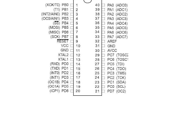
Atmega16 Pin Diagram And Explanation


Atmega16 Pin Diagram And Explanation

• MOSI (Master Out Slave In)
• MISO (Master In Slave Out)
• SCK (Serial Clock)
• RESET
• GND (Ground)
Now connect the power supplies that are Vcc and GND to the micro controller.
Vcc = +5V and GND = 0V
Do not forget to connect Reset to Vcc with a 1K/10K resistor for pulling up. That is it we are ready with the hardware.
ATmega16 has 16 KB programmable flash memory, static RAM of 1 KB and EEPROM of 512 Bytes. 


Pin No.
Pin name
Description
Alternate Function
1
(XCK/T0) PB0
I/O PORTB, Pin 0
T0: Timer0 External Counter Input.
XCK : USART External Clock I/O
2
(T1) PB1
I/O PORTB, Pin 1
T1:Timer1 External Counter Input
3
(INT2/AIN0) PB2
I/O PORTB, Pin 2
AIN0: Analog Comparator Positive I/P
INT2: External Interrupt 2 Input
4
(OC0/AIN1) PB3
I/O PORTB, Pin 3
AIN1: Analog Comparator Negative I/P
OC0 : Timer0 Output Compare Match Output
5
(SS) PB4
I/O PORTB, Pin 4
In System Programmer (ISP)
Serial Peripheral Interface (SPI)
6
(MOSI) PB5
I/O PORTB, Pin 5
7
(MISO) PB6
I/O PORTB, Pin 6
8
(SCK) PB7
I/O PORTB, Pin 7
9
RESET
Reset Pin, Active Low Reset

10
Vcc
Vcc = +5V

11
GND
GROUND
12
XTAL2
Output to Inverting Oscillator Amplifier
13
XTAL1
Input to Inverting Oscillator Amplifier
14
(RXD) PD0
I/O PORTD, Pin 0
USART Serial Communication Interface
15
(TXD) PD1
I/O PORTD, Pin 1
16
(INT0) PD2
I/O PORTD, Pin 2
External Interrupt INT0
17
(INT1) PD3
I/O PORTD, Pin 3
External Interrupt INT1
18
(OC1B) PD4
I/O PORTD, Pin 4
PWM Channel Outputs
19
(OC1A) PD5
I/O PORTD, Pin 5
20
(ICP) PD6
I/O PORTD, Pin 6
Timer/Counter1 Input Capture Pin
21
PD7 (OC2)
I/O PORTD, Pin 7
Timer/Counter2 Output Compare Match Output
22
PC0 (SCL)
I/O PORTC, Pin 0
TWI Interface
23
PC1 (SDA)
I/O PORTC, Pin 1
24
PC2 (TCK)
I/O PORTC, Pin 2
JTAG Interface
25
PC3 (TMS)
I/O PORTC, Pin 3
26
PC4 (TDO)
I/O PORTC, Pin 4
27
PC5 (TDI)
I/O PORTC, Pin 5
28
PC6 (TOSC1)
I/O PORTC, Pin 6
Timer Oscillator Pin 1
29
PC7 (TOSC2)
I/O PORTC, Pin 7
Timer Oscillator Pin 2
30
AVcc
Voltage Supply = Vcc for ADC
31
GND
GROUND
32
AREF
Analog Reference Pin for ADC
33
PA7 (ADC7)
I/O PORTA, Pin 7
ADC Channel 7
34
PA6 (ADC6)
I/O PORTA, Pin 6
ADC Channel 6
35
PA5 (ADC5)
I/O PORTA, Pin 5
ADC Channel 5
36
PA4 (ADC4)
I/O PORTA, Pin 4
ADC Channel 4
37
PA3 (ADC3)
I/O PORTA, Pin 3
ADC Channel 3
38
PA2 (ADC2)
I/O PORTA, Pin 2
ADC Channel 2
39
PA1 (ADC1)
I/O PORTA, Pin 1
ADC Channel 1
40
PA0 (ADC0)
I/O PORTA, Pin 0
ADC Channel 0


Port A (PA7 ‐ PA0): Port A serves as the analog inputs to the A/D Converter. Port A also serves as an 8‐bit bi‐directional I/O port, if the A/D Converter is not used. When pins PA0 to PA7 are used as inputs and are externally pulled low, they will source current if the internal pull‐up resistors are activated. The Port A pins are tri‐stated when a reset condition becomes active, even if the clock is not running.
Port B (PB7 ‐ PB0): Port B is an 8‐bit bi‐directional I/O port with internal pull‐up resistors (selected for each bit). Port B also serves the functions of various special features of the ATmega16 as listed on page 58 of datasheet.
Port C (PC7 ‐ PC0): Port C is an 8‐bit bi‐directional I/O port with internal pull‐up resistors (selected for each bit). Port C also serves the functions of the JTAG interface and other special features of the ATmega16 as listed on page 61 of datasheet. If the JTAG interface is enabled, the pull‐up resistors on pins PC5(TDI), PC3(TMS) and PC2(TCK) will be activated even if a reset occurs.
Port D (PD7 ‐ PD0): Port D is an 8‐bit bi‐directional I/O port with internal pull‐up resistors (selected for each bit). Port D also serves the functions of various special features of the ATmega16 as listed on page 63 of datasheet.
RESET: Reset Input. A low level on this pin for longer than the minimum pulse length will generate a reset, even if the clock is not running.
XTAL1: External oscillator pin 1
XTAL2: External oscillator pin 2
41
AVCC: AVCC is the supply voltage pin for Port A and the A/D Converter. It should be externally connected to VCC, even if the ADC is not used. If the ADC is used, it should be connected to VCC through a low‐pass filter.
AREF: AREF is the analog reference pin for the A/D Converter.


You can see it has 32 I/O (Input/output) pins grouped as A, B, C & D with 8 pins in each group. This group is called as PORT.
• PA0 ‐ PA7 (PORTA)
• PB0 ‐ PB7 (PORTB)
• PC0 ‐ PC7 (PORTC)
• PD0 ‐ PD7 (PORTD)
Notice that all these pins have some function written in bracket. These are additional function that pin can perform other than I/O. Some of them are.
• ADC (ADC0 ‐ ADC7 on PORTA)
• UART (Rx,Tx on PORTD)
• TIMERS (OC0 ‐ OC2)
• SPI (MISO, MOSI, SCK on PORTB)
• External Interrupts (INT0 ‐ INT2)


Related Posts Plugin for WordPress, Blogger...

Popular Posts